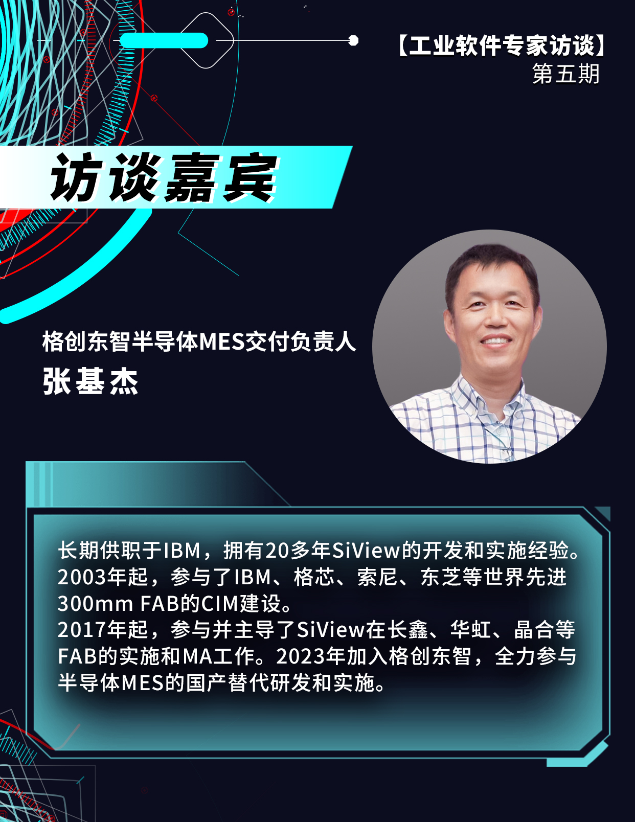
GTRONTEC Industrial Software Expert Interview Fifth Episode: Why is it so difficult for 12-inch Wafer Fab MES to break through?
Currently, China has become the global manufacturing center, with the world's largest industrial output and the most industrial scenarios. In the new round of industrial transformation, smart manufacturing has become the main direction for countries to seize strategic high ground. As a key core technology of smart manufacturing, industrial software plays an important role in promoting industrial digital transformation.
Focus on China's manufacturing 'soft power'
GTRONTEC Industrial Software Expert Interview Fifth Episode
Why is it so difficult for 12-inch Wafer Fab MES to break through?
The following expert interview transcript:
1. The software development of semiconductor CIM/MES is recognized as a highly challenging 'high ground' in the industry. Where is this 'high ground' reflected?
Production industrial software in the semiconductor field is collectively called CIM system. It uses computer control and information processing functions to help semiconductor factories achieve automated production of products.
As a typical technology-intensive tech manufacturing, semiconductor manufacturing has characteristics such as many product types, short cycles, multiple batches, highly complex production processes requiring high precision, fast production updates and information changes, high production costs, and high yield requirements, requiring factories to implement more refined management of the production process.
At the same time, the semiconductor industry chain has many links and long cycles. The CIM system can ensure that each link's equipment executes commands as required, each process parameter has no deviation, each wafer's defects can be traced, and each device is efficiently utilized.
The realization of these links benefits from CIM's four functions: allocation management of production resources and human resources, design functions such as programming and modeling, automated manufacturing functions, and quality control functions. These functions are implemented by different software.
Semiconductor CIM/MES, especially in 12-inch wafer fabs, drives the fully automated control and information flow of the entire production line. Man-Machine-Material-Method-Environment all rely on CIM/MES instructions to execute various detailed decisions. The more complex the semiconductor process automation production flow, the higher the functional requirements for CIM/MES. On an unmanned basis, it is impossible to rely on human eyes to identify production steps or quality, relying on CIM/MES to provide complete functions to handle these production closed-loop management. In addition, semiconductor production costs are high, and there are high system indicators for system stability, performance, and exception handling. These are the biggest challenges of semiconductor CIM/MES.
2. Can the MES of 12-inch wafer fabs be understood as a 'high ground' on top of a 'high ground'? Compared to 6-inch and 8-inch fabs, where is it higher?
Semiconductor from 6-inch, 8-inch to 12-inch, all have different challenges. In addition to the chips produced per wafer, the process flow magnitude increases, requiring higher production process flows, materials, and production management technologies. The use of semiconductor MES systems has evolved from processing station accounting, data collection, basic control, visualization, to detailed control, production anomaly monitoring, event-process human-machine interaction management, and higher levels of automated production lines. As the core brain of 12-inch wafer fabs, MES needs to carry more complete functions and more thoroughly connect various processing links.
8-inch fabs are mainly semi-automatic, while 12-inch are mostly fully automatic. In a 12-inch wafer fab, each wafer circulates among hundreds or even thousands of equipment, with over a thousand production processes. Any error in any link will directly affect yield and efficiency.
A chip needs to go through multiple links and processes such as thin film deposition, photoresist coating, photolithography development, etching, measurement, cleaning, ion implantation, etc. In 12-inch production lines, the processes can even reach two thousand steps. Therefore, the data for each chip in production is very large, and the data volume grows rapidly with process evolution. According to Applied Materials data, a 45nm wafer fab has an annual data volume of about 50TB, while a 28nm fab can reach 80TB, and a 14nm fab has 140TB per year. The collection, flow, and processing of such huge data place extremely high demands on the system.
3. In terms of domestic replacement, the localization of MES for 12-inch fabs still has a long way to go. Why is it so difficult?
Insufficient attention: Compared to chip design software like EDA, CIM systems have always been undervalued. The core MES system in CIM only accounts for 1% of the total investment in a wafer fab. Compared to fabs that cost billions, it is difficult to attract industry attention. Upstream manufacturers prefer to use mature solutions to cope with various problems in production.
High entry barriers: As an industrial software covering all links of wafer production, CIM not only requires developers to have strong software capabilities but also to have a thorough understanding of each production link and seamlessly integrate the two. More difficultly, there are many technical secrets (Know-how) in semiconductor manufacturing, and it is hard to enter this field without being a seasoned industry professional. In addition, semiconductor production processes are extremely complex, requiring 24*7 uninterrupted production. A single downtime can cause wafers to be scrapped, resulting in huge losses. Therefore, FAB factories have extremely high requirements for MES systems and can accept high prices. This makes it difficult for domestic MES to gain opportunities to hone themselves in正规大厂 (正规大厂可能指正规大型工厂).
Small market size: According to Technavio data, the potential market growth share of the entire CIM market (including photovoltaic manufacturing, pharmaceuticals, semiconductor manufacturing, etc.) from 2021 to 2026 is $8.72 billion;另据IDC报告, the overall MES market share in China in 2021 was about 3.81 billion RMB. In this case, the market share细分到半导体 (segmented to semiconductor) may be smaller. However, the 'IDC China Core Industrial Software Market Forecast, 2022-2026' report predicts that the MES software market will grow from 3.81 billion RMB in 2021 to 10.81 billion RMB in 2026, with a five-year compound annual growth rate of 23.2%.
If 12-inch fab MES needs to penetrate the entire production process, it should not only focus on software development technology but more importantly渗透实际半导体加工流程 (penetrate the actual semiconductor processing flow), understand actual business needs (why), and design functions for different processing area scenarios. This requires a process of沉淀经验 (precipitating experience) on an actual factory line.一般人都把这个称为OT (Operation Technology) and IT (Information Technology)的结合 (combination).
Therefore, we also hope that domestic 12-inch wafer fabs can provide more opportunities for domestic systems to be validated on production lines. If domestic fabs only follow foreign large厂 systems and experiences, the path for domestic 12-inch MES will be more difficult.
4. As an MES supplier, what abilities are most important in the implementation of 12-inch fab MES projects?
Personally, I think first, have a good product foundation, have certain semiconductor industry沉淀 (precipitation) and stably对应多产品 (correspond to multiple products) (high mix product),高产能 (high capacity) scenarios. Second, the project implementation team needs to have experience in semiconductor production line business and can guide customers to correctly use the system and jointly promote production line KPIs. In addition, the overall project implementation execution process (Project Management) and user's active cooperation are also important links.
5. Can you combine your work experience to talk about, what do you think are better paths for the 'breakthrough' of domesticization of 12-inch wafer fab MES?
12-inch wafer fabs need a complete CIM, with MES combined with different modules, such as SPC, EAP, RTD, FDC, APC, etc., to exert overall control.
Rather than a breakthrough, it is better to say that everyone leverages various strengths: on an innovation platform, launch a more complete solution; in different production lines and processes, implement the combination of process and system technology to solve foreseeable and future challenges of the production line. Foreign large companies like IBM, AMAT, Daifuku, camLine, Siemens have actual project cooperation cases, supporting processes such as SOI, SiC, IGBT.
But in China, each is developing all modules. In the situation of domestic experienced personnel shortage, to independently complete all systems, especially MES, need to establish a true elite team, devote to R&D.
6. Why did you choose to join GTRONTEC? What are your plans next?
GTRONTEC, as a young company, started with TCL's support, and has continuously expanded its business scope inside and outside the group over the past 5 years, achieving leapfrog progress. While covering the full spectrum of traditional businesses, GTRONTEC focuses on deeply cultivating the semiconductor industry, including the comprehensive combination of smart hardware and CIM, committed to developing independently controllable 12-inch MES and peripheral systems. GTRONTEC originated from semiconductor manufacturing, with deep semiconductor genes as support, and can be said to be more comfortable in the R&D of new CIM products. For over 20 years, I have focused on the development and delivery of semiconductor CIM at IBM, and now I also hope to contribute to the development of domestic CIM. Therefore, joining GTRONTEC is also finding an excellent opportunity to leverage my and the team's abilities.
The R&D and implementation of semiconductor CIM require the cooperation of a large excellent team. I hope to work with the R&D team to go all out and spend two years to polish the product. At the same time, I will lead the delivery team to do a good job in customer delivery services, fully investigate customer needs, promote product R&D, and strive to build our own CIM total solution with the strength of GTRONTEC's people in a short time.