Success Story|GTRONTEC AOI Inspection Equipment Helps Leading Silicon Wafer Manufacturer Achieve Full-Process Automated Quality Inspection

A leading domestic semiconductor materials manufacturer, specializing in the R&D and production of semiconductor silicon wafers and related industries, is committed to innovation-driven development and provides comprehensive product solutions for global customers.
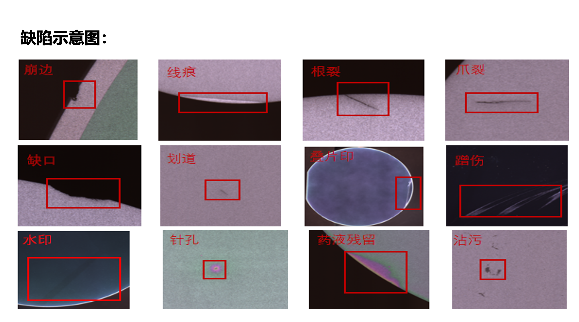
As is well known, silicon wafers are critical materials for producing integrated circuits, discrete devices, sensors, and other semiconductor products, forming a foundational part of the semiconductor industry chain. However, during silicon wafer production, the complex processes generate numerous and varied defects. Most factories rely on manual visual inspection for appearance checks, which poses several drawbacks as production capacity increases and process requirements become more stringent:
- Inconsistent judgment standards, low inspection efficiency
- High turnover of quality inspectors, long training cycles
- No archival records, inability to trace historical data
- Multiple defect types, inability to quantify defect statistics
- Unable to monitor and feedback data in real-time, lacking process anomaly identification
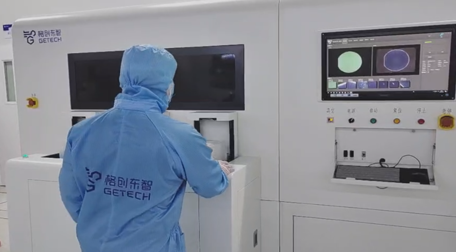
GTRONTEC, in line with the production processes and product characteristics of silicon wafer manufacturers, introduced the ALIOTH series S800P product. This product specializes in automated detection, classification, and statistics of various defects during processes such as acid etching, polycrystalline, back sealing, and edge removal. Utilizing CV+AI composite algorithms, it significantly improves defect detection accuracy, enhances quality control during silicon wafer production, and helps factories reduce costs and increase efficiency.
1) Product appearance defect detection: Uses machine vision to capture surface feature images, precisely locates and captures defects in the images, and accurately identifies and classifies them;
2) Data statistical analysis: Analyzes the proportion of defect types, accurately locates defect positions, and identifies directions for process improvement; conducts batch statistical analysis of defect patterns to pinpoint causes and processes responsible for defects, and monitors equipment and process performance fluctuations in real-time; combines defect data and trend information from the production process to perform root cause analysis for improving manufacturing processes and optimizing production workflows;
3) Adaptive defect recognition: Through adaptive imaging configuration adjustments and multiple imaging methods, combined with unsupervised transfer learning AI algorithms, achieves adaptive detection of new defect forms regardless of size or shape. Coupled with automated quality monitoring, it alerts to equipment issues.

To meet customer quality control requirements, the company adopted the ALIOTH-S800P AOI appearance defect detection equipment to replace traditional manual visual inspection. This enables automated defect detection, classification, statistics, and grading during silicon wafer production, greatly improving inspection efficiency and accuracy.
1. Labor input reduced by 80%
By replacing manual inspection with automated equipment, each silicon wafer is inspected in 10 seconds, significantly boosting efficiency to meet high production demands; one person can maintain multiple devices simultaneously, greatly reducing labor input and shortening training cycles.
2. Defect detection accuracy reaches 99%
Utilizes adaptive high-resolution imaging to stably capture product image features and establishes unified defect detection standards with machine vision, effectively enhancing the stability and accuracy of defect detection.
3. Shipment yield increased by 20%
While performing defect detection, extensive data statistical analysis helps identify front-end process issues and improvement directions, thereby promoting process optimization. Combined with precise product grading, this leads to higher shipment yields.