October 25-27, the 21st China Semiconductor Packaging and Testing Technology and Market Annual Conference was held in Kunshan. The theme of this annual conference is 'Dare to be First, Seeking New Development in the Packaging and Testing Industry'. Over 2,300 industry experts, scholars, and government leaders from around the world gathered to discuss hot topics such as China's semiconductor industry policies and development directions, advanced packaging and testing technologies, packaging and testing equipment, and intelligent manufacturing. Ma Wei, Deputy General Manager of the Semiconductor Business Unit of GTRONTEC, was invited to attend and deliver a keynote speech, sharing construction ideas and solutions for semiconductor packaging and testing 'lights-out factories'.
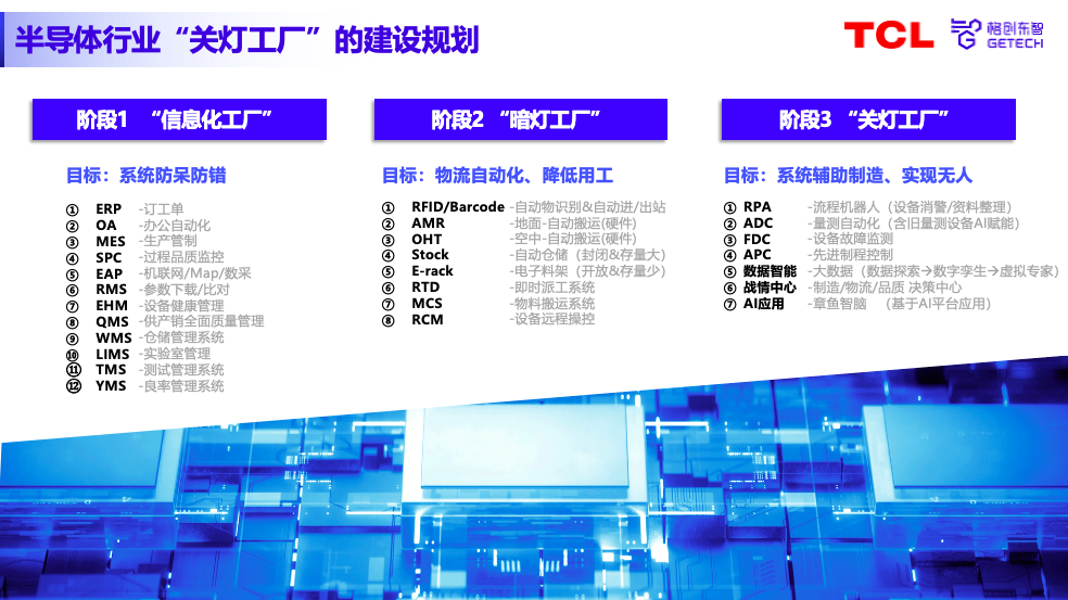
 Ma Wei introduced that in advanced manufacturing industries like semiconductors, the construction planning of 'lights-out factories' generally includes three steps: first, 'informationized factory', achieving system error prevention through basic equipment information acquisition and control; second, 'dark factory', reducing labor through automated material handling; third, 'lights-out factory', using big data, AI, and other technologies to achieve system-assisted manufacturing, unmanned operations, and other goals, helping factories upgrade from informatization to reduced manpower, then to unmanned and intelligent digital transformation.Therefore, for the system construction planning of semiconductor packaging and testing smart factories, we recommend a three-phase approach: Phase 1, use applications like MES, EAP, SPC to get the production line running; Phase 2, achieve quality control and yield improvement through automated material handling systems and quality management systems, including RTD, QMS, FDC; Phase 3, use advanced applications like big data and AI to achieve perfect line balance.
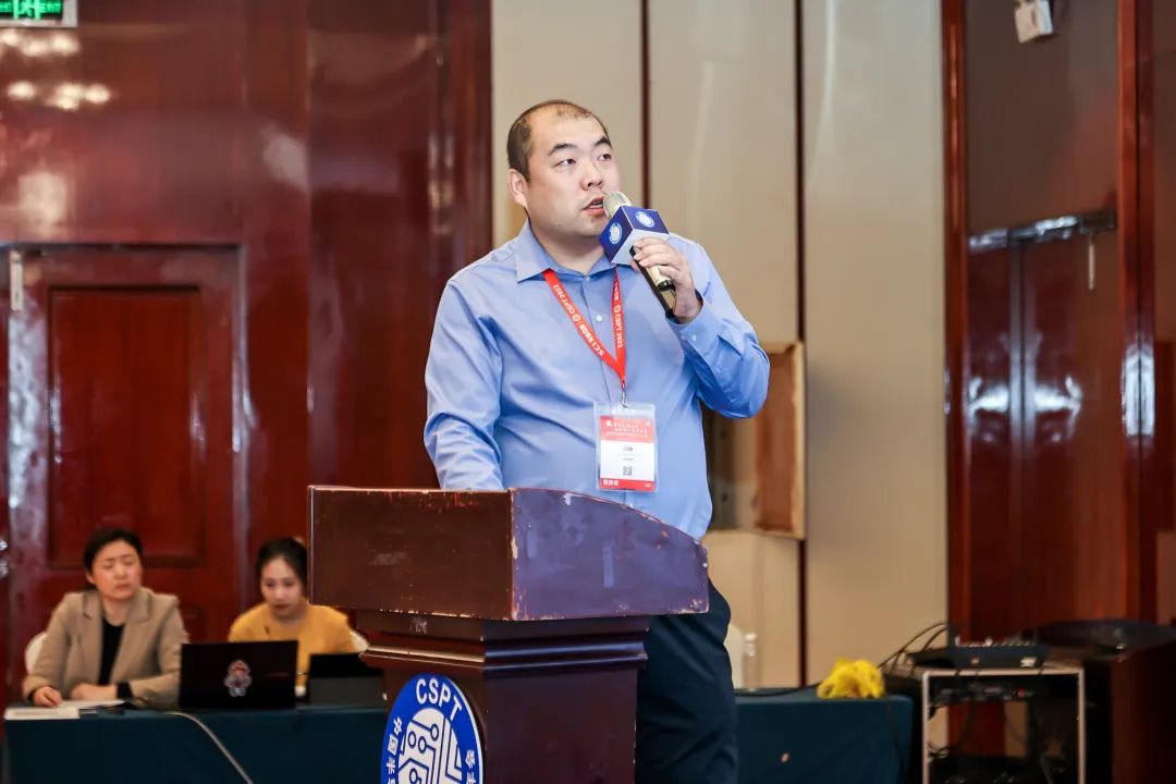 "Before building a 'lights-out factory', companies need to assess the construction scope based on their own situation. Choose different solutions at different stages." Ma Wei said, generally, Phase 1 construction should prioritize sites with high benefits and low transformation costs, such as sites where labor costs can be reduced by over 80% or manpower reduced by more than 50 people; other sites can be addressed in Phase 2 to complete the full line; Phase 3 can use applications like big data and AI to achieve system-assisted management at the workshop team level.
Additionally, Ma Wei focused on key points such as material identification, handling methods, WIP stacking, and machine control, detailing the specific construction plans for logistics automation in semiconductor packaging and testing 'lights-out factories' at Wafer thinning-dicing, bonding, oven, singulation-final inspection-FT stations. He pointed out that as a software company born from semiconductor manufacturing, GTRONTEC has deep understanding of semiconductor industrial sites,积累了大量的半导体生产Know-How,能够辅助企业炼好“内功”,避免走弯路。 (Note: '积累了大量的半导体生产Know-How,能够辅助企业炼好“内功”,避免走弯路' translates to 'accumulated extensive semiconductor production know-how, able to assist companies in strengthening their internal capabilities and avoiding detours.')
 Based on a new perspective of 'production-analysis-prediction', GTRONTEC has built a full-stack domestic CIM overall solution for semiconductor smart factories, achieving transparent production execution, automated equipment management, efficient plan coordination, accurate quality traceability, and logistics management, helping semiconductor companies increase capacity, reduce losses, improve yield, and optimize production and process design.For example, in production intelligence, for the semiconductor industry, how to effectively and quickly mine value from massive data is key to intelligent manufacturing development. GTRONTEC, based on innovations in data big models, has achieved high intelligence in semiconductor business, able to use equipment and business data to drive root cause定位,前置预警,反控优参与自动决策,实现闭环管理,为半导体工厂提供一站式、一键式、可协作共享的数据科学解决方案和工具平台。 (Note: 'root cause定位,前置预警,反控优参与自动决策,实现闭环管理' translates to 'root cause定位 (root cause定位),前置预警 (proactive warning),反控优参与自动决策 (feedback control optimization and automatic decision-making), achieving closed-loop management, providing semiconductor factories with one-stop, one-click, collaborative and shareable data science solutions and tool platforms.')
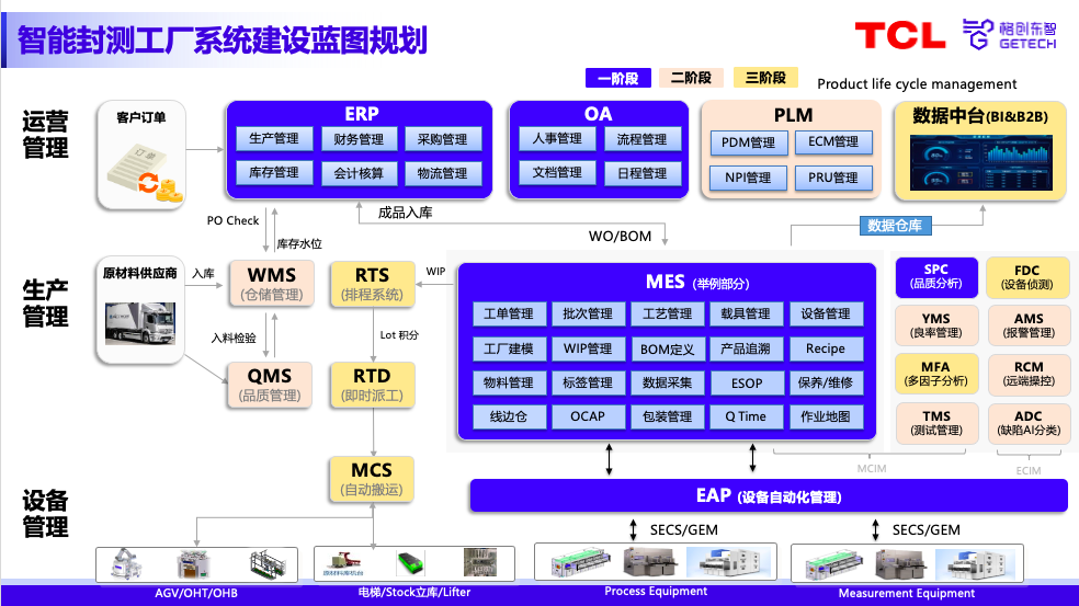
In digital quality solutions, GTRONTEC has a complete product and service matrix, including QMS quality management system (ranked 7th in all domestic industries and 1st in the semiconductor industry), SPC statistical process control, FDC fault detection and classification, MFA multi-factor analysis, ADC intelligent visual inspection, etc., helping packaging and testing factories effectively improve quality management and solve yield management challenges.Currently, GTRONTEC has successfully served semiconductor industry clients such as SMIC, SAIC Infineon, Wuhan Xinxin, Zhuzhou CRRC, Yangjie Technology, and Ideal Auto-Scott Semiconductor.