Coverage of the Packaging and Testing Annual Conference: GTRONTEC Shares Domestic CIM Solutions for Advanced Packaging
2024-09-27
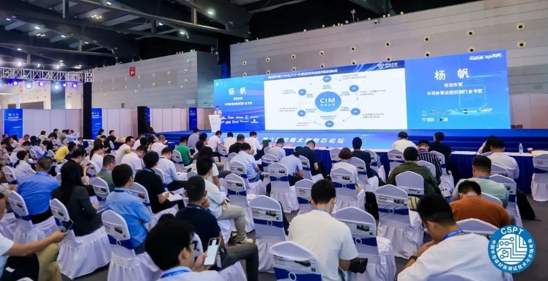
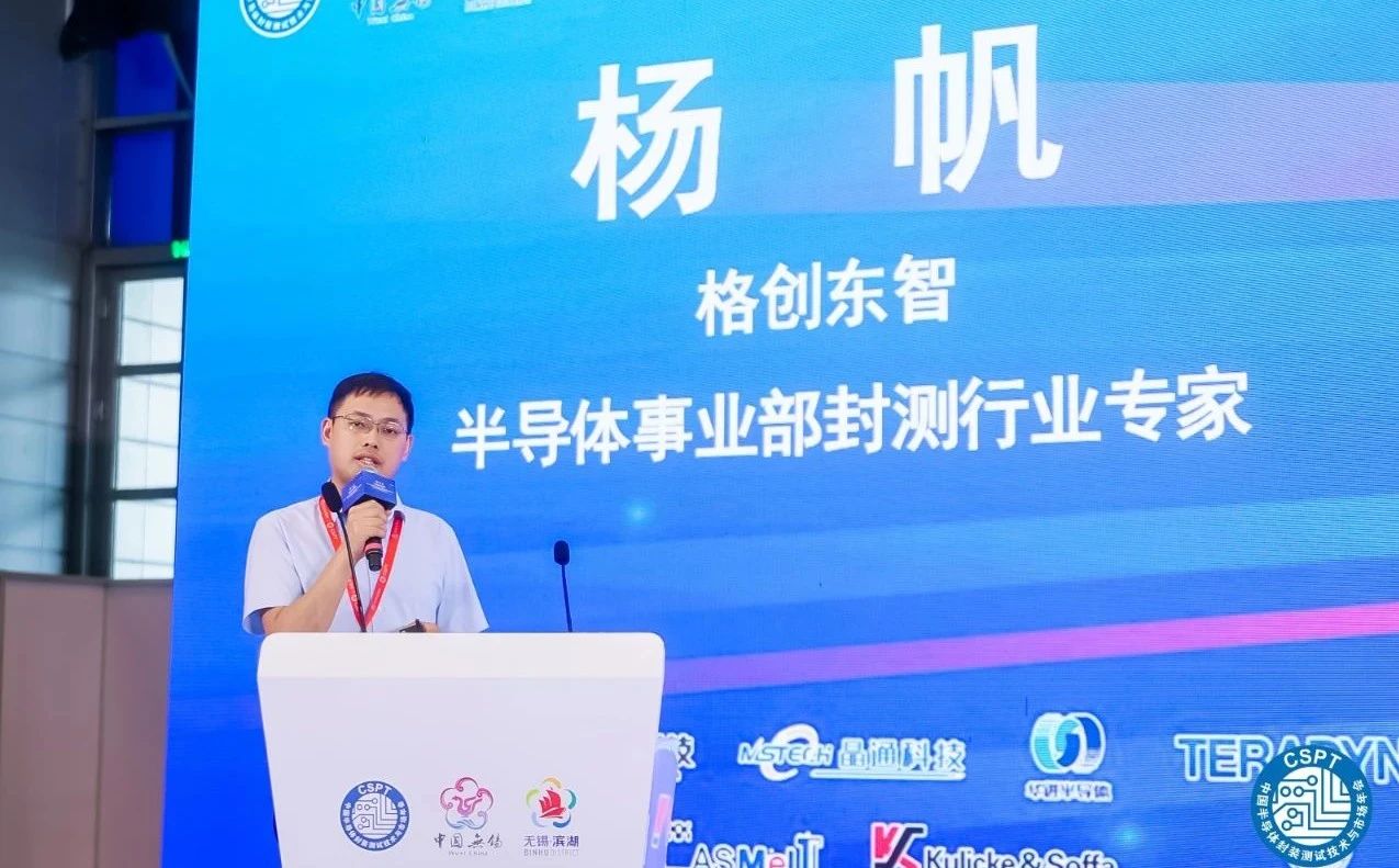
Recently, the 22nd China Semiconductor Packaging and Testing Technology and Market Annual Conference - the 6th Wuxi Taihu Core Innovation Forum, a bellwether for the integrated circuit industry, was successfully held in Wuxi, Jiangsu. The conference brought together discussions on hot topics such as advanced packaging technology, processes, equipment, key materials, innovation, and investment, offering attendees a feast of ideas. On the afternoon of September 25, Yang Fan, an expert in the packaging and testing industry from GTRONTEC's Semiconductor Business Unit, was invited to speak at the Advanced Packaging and Testing Technology Forum, delivering a keynote speech titled "Domestic CIM Helps Advanced Packaging Meet Challenges and Opportunities", contributing domestic CIM solutions for advanced packaging to the industry.
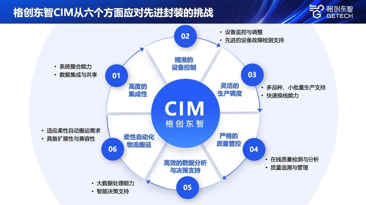
As widely known in the industry, semiconductor chips undergo two major processes: "front-end" wafer manufacturing and "back-end" packaging and testing. In recent years, driven by demands such as AI and HPC, advanced packaging has emerged, meeting the needs for high-density packaging with more pins, smaller chip systems, and higher integration. This not only significantly enhances chip performance but also greatly reduces the threshold and cost of wafer manufacturing. Unlike traditional back-end packaging and testing processes, advanced packaging lies in the crossover area between wafer manufacturing and packaging and testing, forming a unique "mid-end" process. It is predicted that by 2025, China's advanced packaging market will reach a scale of hundreds of billions, with a market share exceeding 50% for the first time, surpassing traditional packaging.In response, as an industrial intelligence solutions provider deeply rooted in the pan-semiconductor industry, GTRONTEC has already made early preparations. To meet the special management requirements of the "mid-end process" in advanced packaging, GTRONTEC has independently developed and launched G-MES 3.0 based on the back-end G-MES 1.0 and front-end G-MES 2.0: not only does it share a data foundation with G-MES 1.0 & 2.0 (enabling upgrade and expansion across different versions), but it also adds numerous features tailored to the special needs of advanced packaging. Additionally, G-MES 3.0 excels in data integration and data sharing, enabling the connection of multiple systems, effective integration and sharing of diverse data, achieving consolidation of multiple systems, and customized functional expansion. Based on these new technological developments, GTRONTEC can tailor a complete set of G-CIM overall solutions for advanced packaging customers.
In terms of specific applications, Yang Fan further explained that this solution features flexible modeling methods supporting small-batch trial production; multi-dimensional monitoring of equipment CMK, enabling immediate alerts for equipment capability deviations; reducing Wafer bond waste through Smart Bond. For some advanced packaging customers facing challenges such as long process chains and complex quality improvements when adopting a full-process vertical industry chain, GTRONTEC can provide full-process quality management system construction services from product development and mass production to quality improvement and after-sales support.
Looking back at GTRONTEC's track record in the semiconductor field, it has successfully helped dozens of semiconductor customers complete hardware and software project deliveries with 0 delays, 0 unfinished projects, and a 100% delivery success rate. This capability stems from the company's strong talent accumulation and R&D investment. To date, GTRONTEC's Semiconductor BG has gathered industry experts from leading semiconductor companies at home and abroad, supported by a team of 400+ semiconductor-specific talents and a resource pool of 500+, with R&D accounting for over 50% of related efforts.In the future, GTRONTEC will continue to focus on the R&D and innovation of industrial intelligence solutions for the entire semiconductor industry chain, benchmark against international leading manufacturers, continuously improve its product system, accelerate scenario intelligence, and stand in the first tier of domestic semiconductor CIM.