GTRONTEC CTO MK Koh: From Experience-Driven to Intelligent Decision-Making, Embarking on a New Journey of Semiconductor AI
Currently, the semiconductor industry is at a critical juncture of intelligent transformation. At the "Large Model × Agent: Semiconductor AI Manufacturing Evolution" seminar hosted by GTRONTEC on March 26, GTRONTEC CTO MK Koh, based on R&D insights from hundreds of semiconductor factories worldwide, deeply analyzed the path of AI technology transitioning from an "auxiliary tool" to a "decision-making hub" and proposed a future-oriented technological reconstruction framework, providing professional insights for semiconductor R&D innovation talents.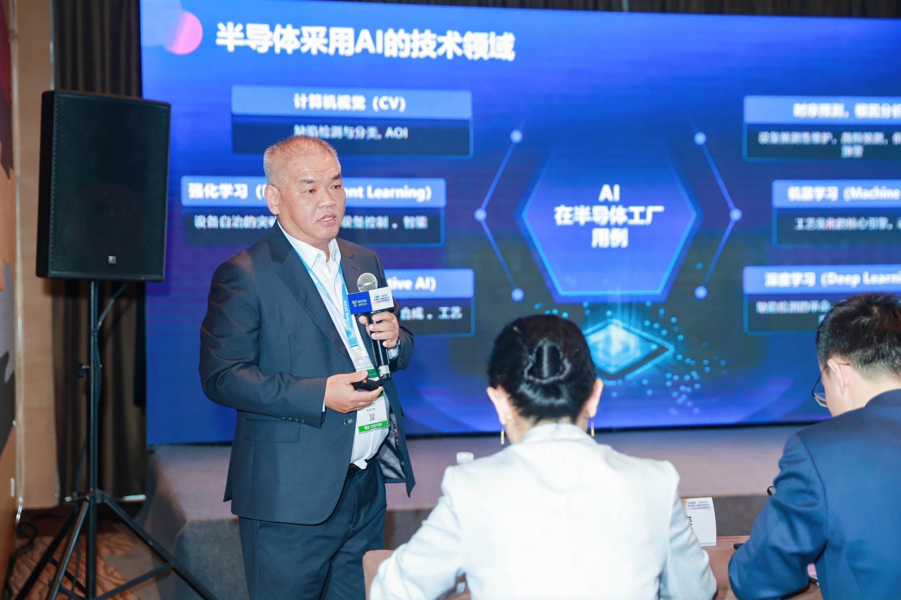
GTRONTEC CTO MK Koh (first from left)
According to MK, over the past 10 to 20 years, digital innovation in the semiconductor industry has improved automation levels by deploying systems such as MES (Manufacturing Execution System), SPC (Statistical Process Control), and APC (Advanced Process Control). In the last 5 to 8 years, AI technology has been widely applied in the semiconductor field, focusing on reducing manufacturing system fluctuations, minimizing engineering system variations, and providing services such as predictive control, big data analysis, optimal PM scheduling analysis, multi-variable parameter analysis, and equipment predictive maintenance. Statistics show that over the past 5 years, 51% of semiconductor investments in AI have been directed toward automation, with relatively lower investments in intelligent equipment control, emphasizing improvements in production line efficiency metrics.
After achieving automation capabilities, more advanced challenges have emerged. He summarized them into five categories: First, defect management constraints, where manual re-inspection after defects occur is costly. Second, yield ramp-up challenges, where yield improvements are difficult during new factory, production line, or process stages, overly relying on external experts or experienced engineers. Third, equipment management dilemmas, where complex equipment parameters and configurations make it hard to fully control, leading to equipment "black-boxing." Fourth, talent gap issues, where technical experts aged 50 and above account for up to 60%, posing challenges for knowledge transfer. Fifth, insufficient supply chain resilience, with many risks arising from material restrictions and policy impacts.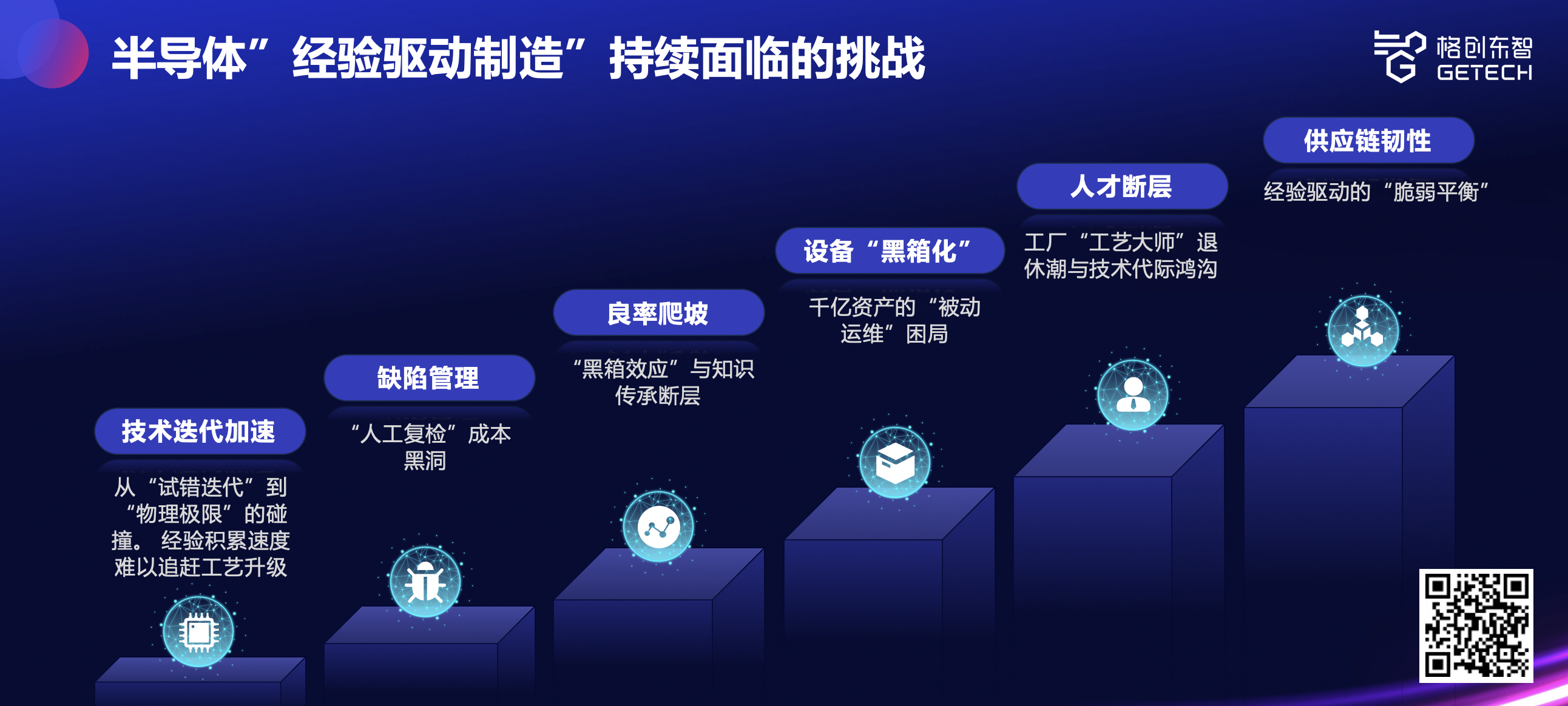
MK suggested that the semiconductor industry should leverage AI to address these challenges and move beyond the "experience-driven" bottleneck. He predicted that AI applications in semiconductor factories are diverse. For example, (1) computer vision technology can be applied in back-end processes, SMT Line, AOI equipment inspection, and inventory-shipping scenarios; (2) time-series prediction technology can be used for equipment predictive maintenance and risk warnings; (3) machine learning technology can optimize equipment parameter adjustments, task assignment, and route optimization; (4) deep learning technology can aid in more effective engineering analysis and equipment repair; (5) generative AI technology can be used to integrate missing data, production fluctuations, and virtual data for new processes/MPI/new product debugging.
However, there remains a gap between technology and application. Promisingly, the emergence of large model technology will bring about four stages of change for the semiconductor industry.
Stage 1: Enhanced user experience. Factories can achieve dialogue with systems, equipment, engineering, and processes through equipment or engineering assistants to understand equipment details. Some companies use virtual glasses for equipment maintenance, opening the "black box" of equipment in virtual mode to grasp parameters and potential issues.
Stage 2: Efficiency tools. Along with improved user experience, corresponding tools enhance efficiency, such as better equipment and process coordination, production chain traceability, and virtual assistants, helping engineers handle multiple tasks like equipment monitoring and issue resolution.
Stage 3: Knowledge accumulation. He emphasized that knowledge accumulation is critical. Given the talent gap in the semiconductor industry, AI should be used to accumulate all production experience, deriving insights from data. By establishing engineering "digital apprentices" that learn from seasoned experts in equipment maintenance and new product debugging, experience can be systematized and engineered, allowing phase-two production lines to apply phase-one experience. Additionally, product equipment should also have corresponding knowledge bases.
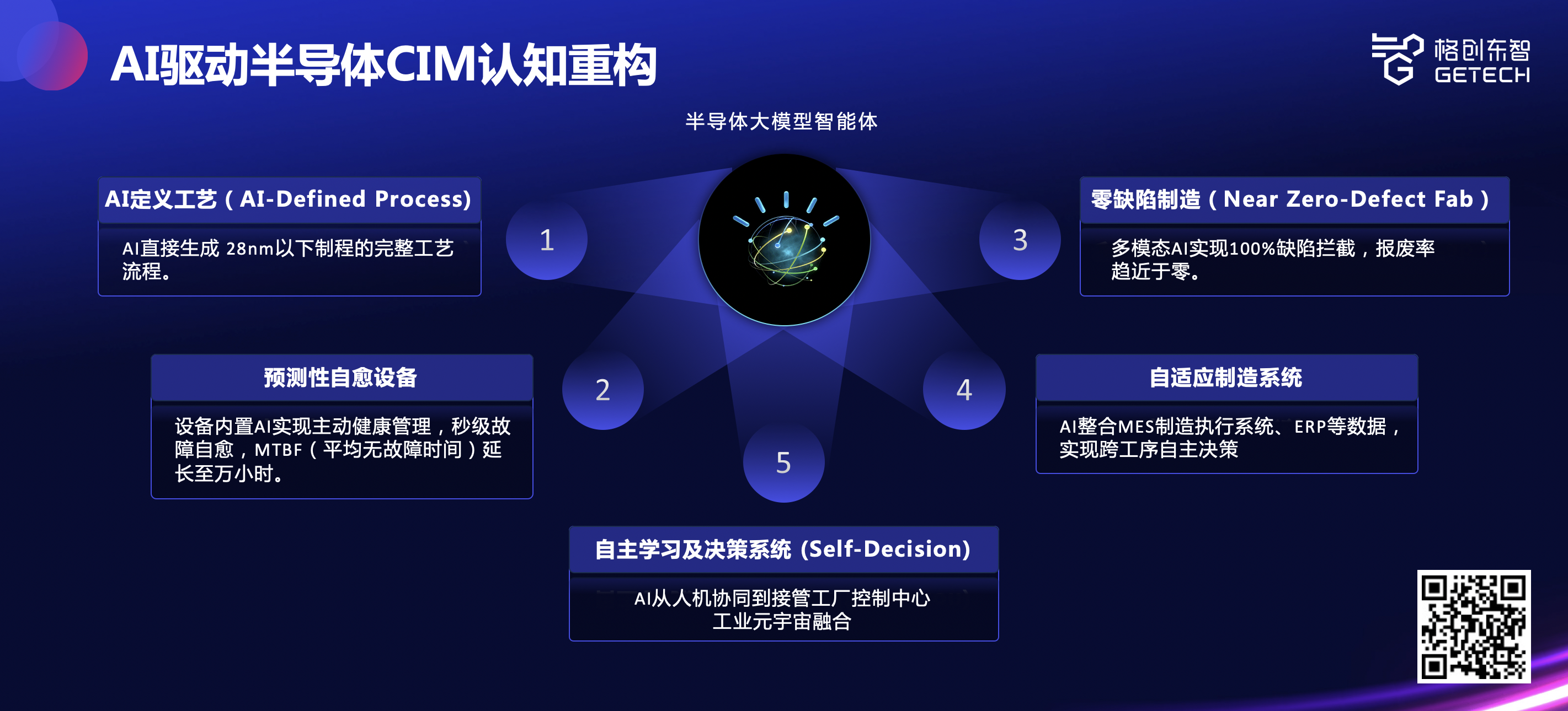
Stage 4: Innovative value. After completing the first three stages, focus should shift to ROI and project value, transitioning from "process catch-up" to "defining future processes," and from "standardized mass production" to "on-demand intelligent manufacturing." Breaking manufacturing silos, AI can enable factory control centers to self-develop, self-learn, self-decide, and even take over factory operations.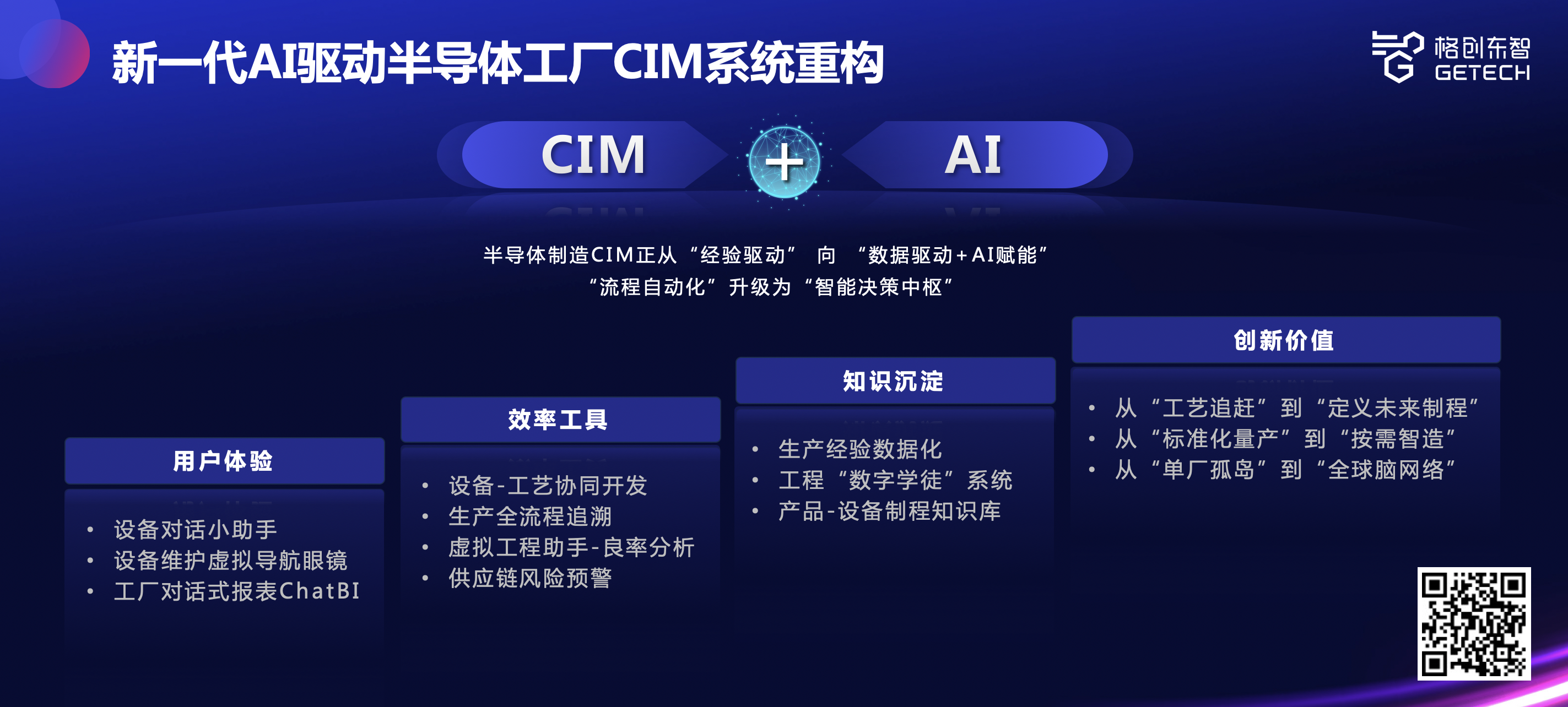
Thus, large model technology is expected to create six major values. First, AI-defined processes, through intelligent agents linking stations and key processes, can potentially achieve near-100% yield. Second, manufacturing systems can transition from passive management to adaptive, self-adjusting, self-repairing, and self-monitoring predictive management, helping extend MTBF (Mean Time Between Failures) goals multiple times. Additionally, factory R&D directions and future designs will possess self-learning and decision-making capabilities, enabling self-development, self-learning, self-decision-making, and even taking over factory operations without human intervention.
However, when applying AI in production lines, visible problems are traditionally solved using historical experience. Now, new AI technologies, especially large model agents, can address invisible and unprecedented issues. From a defect prevention perspective, they generate value through unknown knowledge and intelligent information, shifting from post-event handling to proactive defect prevention—a concept inspired by Professor Jay Lee. In the future, the semiconductor industry is expected to develop large model agents with cognitive generalization, autonomous decision-making, tool operability, and continuous evolution, becoming super tools.
Currently, GTRONTEC has achieved significant results in AI applications for the semiconductor industry. For example, the Chat Insight agent solution, based on a Multi-Agent architecture, supports ChatBI development and handles both structured and unstructured data. It addresses issues like semantic understanding, data dictionary linking, and irrelevant dialogue responses. By building a dual-engine knowledge base, it enables natural language interaction, automatically generating reports and conducting analyses based on user queries (e.g., obtaining root cause analysis of yield issues through dialogue), providing users with a new experience and accumulating new insights and knowledge.
Another solution, AI-FDC Machine Insight, enables equipment intelligence and automatic fault prediction. It uses FTA to manage the entire model, capturing column fluctuations, identifying unknown issues, and entering a self-supervised learning mode. It also reduces pre-training data volume, minimizes debugging efforts, and collaborates with factories to build expert databases.
Additionally, the AI-EAP Equipment Intelligent solution drives equipment automation, not only managing equipment communication but also providing new interaction modes. It reduces the need for engineer assistance by enabling users to analyze equipment composition and perform automatic parsing. Through AI dialogue, it pinpoints issues and establishes equipment knowledge graph engines, improving equipment management efficiency.
MK predicted that the next one to two years will be a turning point for the semiconductor industry's transition from experience-driven to intelligent decision-making centers, achieving data-driven, AI-empowered transformation. Meanwhile, whether in CIM or PEE, work will become increasingly interesting, bringing many innovations and discoveries. AI will not dominate alone; instead, ecosystem collaboration will be essential for the AI reconstruction of semiconductor CIM.
This transformation requires not only algorithmic breakthroughs but also engineers transitioning from "experience holders" to "rule designers." GTRONTEC is committed to collaborating with the industry to build a new semiconductor AI ecosystem and welcome the true arrival of the intelligent decision-making era.