Another 'Excellent Level' Factory Lands, AI Digital Employee GTRONTEC Tianshu Plays a Key Role
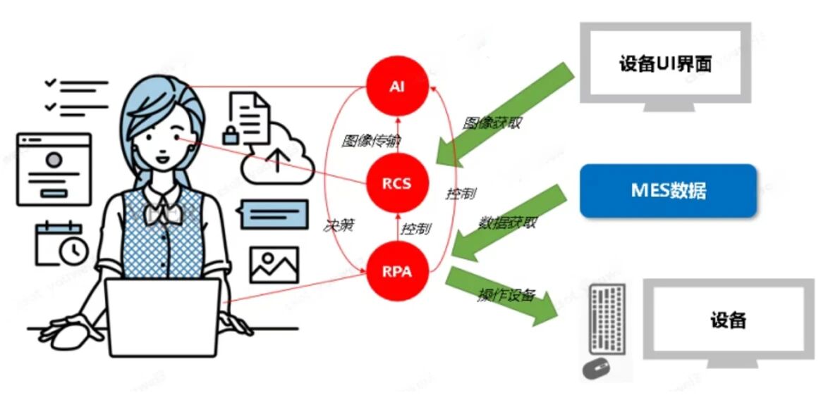
Recently, Suzhou TCL CSOT won the Ministry of Industry and Information Technology's certification for the '2025 Excellent Level Intelligent Manufacturing Demonstration Factory' with its 'AI-driven new display panel smart factory', indicating that it has reached the leading level in China. Entering TCL CSOT (Suzhou)'s 540,000 square meter production plant, highly automated robotic arms and overhead transport tracks operate orderly, with few workers visible. The core supporting the factory's efficient operation is a smart operational system with self-decision and self-execution capabilities, a star intelligence model that accelerates product innovation from the source, and AI digital employees acting as the 'eyes' and 'brain' of quality inspection engineers.
In the key step of micron-level defect inspection for factory products, AI digital employees operate through a closed-loop 'ADC+ADR' dual-system: the ADC Automatic Defect Classification System relies on AI visual technology to automatically identify and classify over 4,000 types of micron-level defects with 95% high accuracy; the ADR Automatic Defect Repair System, upon receiving instructions, drives high-precision tools to perform fully automatic repairs on repairable defects. This system replaces over 75% of traditional manual labor, upgrading the traditional 'human eye + experience' model to a precise and efficient new paradigm of 'AI + data'.
Compared to traditional AOI equipment, which relies on manual re-judgment with misjudgment rates as high as 60%-70%, the digital employees based on the 'ADC+ADR' dual-system are driving the arrival of the 'super intelligent era' in industrial quality inspection. Behind all this is the deep application of GTRONTEC's self-developed Tianshu AI ADC visual inspection system (hereinafter referred to as Tianshu AI). GTRONTEC's Tianshu AI encapsulates the complex computations and operations involved in deep learning into ready-to-use productivity tools, bringing significant efficiency improvements, considerable cost savings, and precise defect identification capabilities through 'millisecond-level re-judgment', redefining 'quality inspection':
1) From 'mass manual re-judgment' to 'AI second-level judgment'. Traditional AOI automatic optical inspection equipment, which can improve initial inspection efficiency, still has misjudgment rates as high as 60%+, requiring substantial manual input for image re-judgment. Re-judgment personnel take an average of 2-3 seconds per image, with high costs, low efficiency, and susceptibility to fatigue and experience differences leading to quality fluctuations.
2) Breaking the limits of the human eye: The panel industry has over 120 types of defects, requiring hundreds of inspectors to judge millions of images daily. Limited by inherent bottlenecks such as eye fatigue, experience differences, and inconsistent standards, the human eye's limitations result in only 85% accuracy. In semiconductor wafer inspection, the system can identify 0.2-20μm macro defects, far exceeding the detection limits of traditional manual or rule-based algorithms.
3) Reducing quality inspection costs: The trial-and-error costs in the pan-semiconductor industry involve equipment processes and bidirectional measurement of techniques, with single defect omission losses potentially reaching tens of millions.
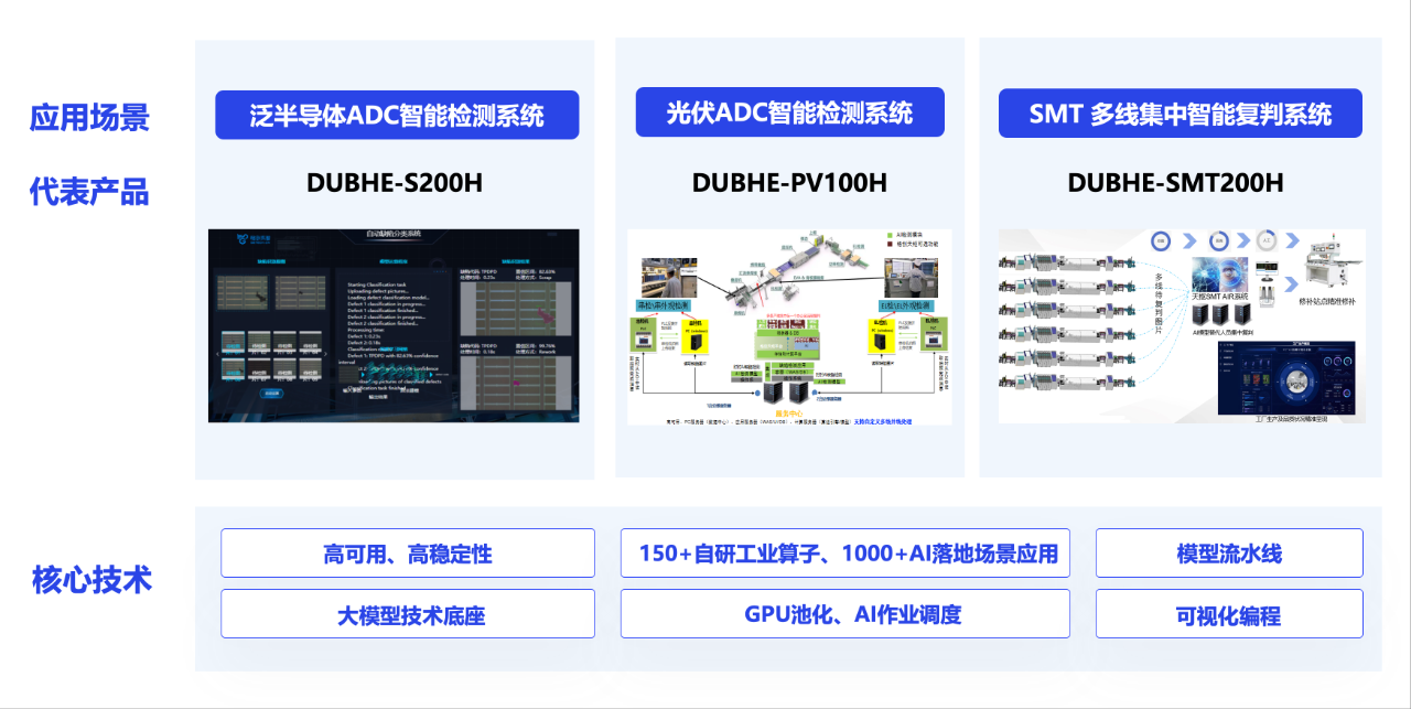
For pan-semiconductor enterprises, quality inspection remains a critical checkpoint related to efficiency and reliability. With the rapid evolution of AI technology, ADC has become the core engine for improving quality and efficiency in manufacturing. GTRONTEC's self-developed Tianshu AI, with its integrated 'Sensing-Storage-Computing-Knowledge' technical architecture, serves as the 'sensory' weapon in this transformation. Through the collaboration of the 'Training-Inference-Scheduling' three modules, it achieves full-process reconstruction of industrial quality inspection.
- Training platform: Built-in tens of millions of defect feature libraries, supporting low-code model iteration.
- Inference platform: Equipped with lightweight edge computing boxes, single image processing speed reaches millisecond level, 5-10 times faster than the human eye.
- Resource scheduling: Dynamically allocates GPU computing power, achieving concurrent operation of 100+ algorithm models at TCL CSOT.
Based on deep insights into the pan-semiconductor industry's needs for defect detection accuracy, speed, and consistency, GTRONTEC addresses common pain points such as low inspection efficiency, high labor costs, and difficult data tracing through multi-module collaborative architecture design, building an industry-leading optical laboratory. The equipment covers visual inspection imaging needs for 30+ industries. Breakthroughs have been achieved in optical solutions for imaging materials with transmittance, reflectivity, and absorbance, with multiple optical imaging patents applied for, greatly reducing optical imaging technology and algorithm detection indicators. This accelerates customers' experience of triple leaps in quality inspection: 'millisecond-level re-judgment efficiency, over 95% detection accuracy, and cost reduction through model self-training and data self-governance', outperforming competitors with comprehensive advantages.
- Faster production cycle: No reference photos needed, capacity doubled, production more efficient.
- Strong system compatibility: Supports mixed multiple image types, meets diverse inspection needs, offers greater choice freedom.
- Fast, accurate, and stable detection results: Quickly uploads classified results to yield systems, enabling timely access to inspection results, quick decision-making, and improved production efficiency.
- More flexible services: Customizes models based on pan-semiconductor enterprise needs, aligning with unique production processes and yield requirements.
- Faster response: Quickly responds to customers anytime, formulates improvement plans, ensures timely problem resolution.
- Lower expansion costs: Software can be sold separately, reducing enterprise expansion costs, allowing flexible business scaling.
- Strong price competitiveness: Obvious advantages in price and maintenance fees, providing cost-effective solutions, lowering operational costs.
This technological maturity is not accidental. It stems from years of continuous investment and interdisciplinary integration in industrial vision, optical design, precision machinery, and control algorithms. Currently, Tianshu AI has been successfully applied in 1000+ industrial scenarios, validated by the landing of the Excellent Level Intelligent Manufacturing Demonstration Factory, with accumulated billions of defect data providing strong support for model and data self-training and self-optimization.
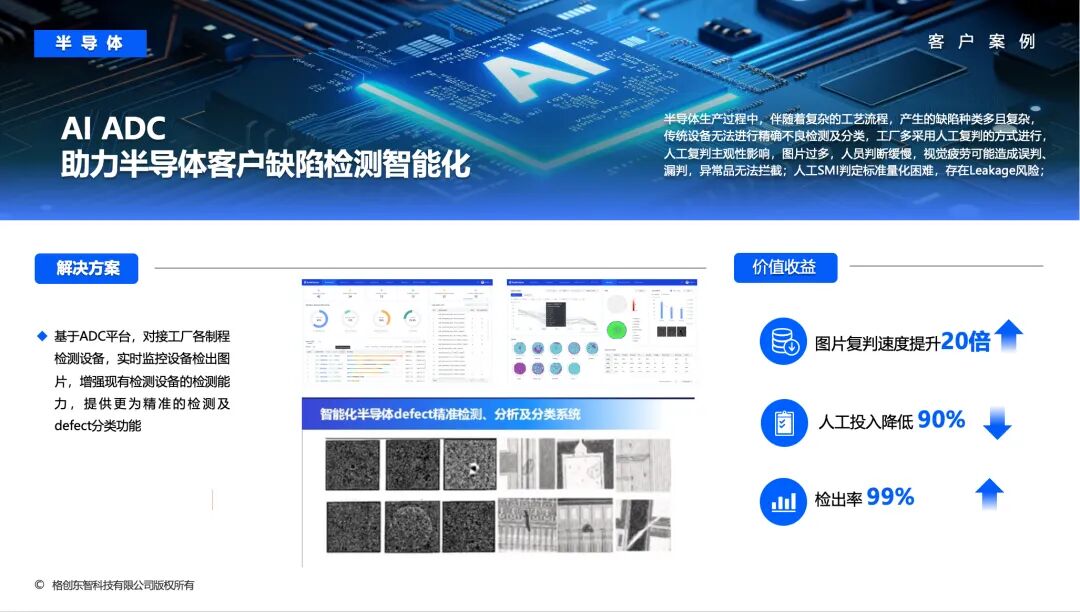
Notably, the company has numerous typical cases in the semiconductor, semiconductor display, and SMT industries. In a semiconductor production project, it helped a client reduce labor input by 90%, with defect detection rates exceeding 99%.
The success of TCL CSOT (Suzhou)'s AI digital employees is the best footnote to GTRONTEC's industrial quality inspection practices. Currently, the company is actively promoting industry-academia-research collaboration, partnering with TCL Industrial Research Institute to strengthen capabilities in complex defect pattern discovery and cross-domain knowledge transfer.
In the future, as chip sizes continue to shrink and new display technologies accelerate iteration, industrial inspection will evolve towards higher precision, faster response, and stronger generalization. GTRONTEC will serve as a key cornerstone in building China's industrial intelligence system, redefining the role of 'quality inspection' in manufacturing—from passive to preventive, from experience to intelligence-driven—helping Chinese pan-semiconductor enterprises win in global competition with 'intelligence'.